OLED Burn In on Devices
The Problem
OLED is a beautiful technology. It gives us incredible contrast in electronic displays, LCD equivalents look poor in comparison, and even VA panels don't get close - but they come with a risk, the dreaded pixel burn-in.
OLED pixels reduce their brightness throughout their life through use. If you have displays with static content (i.e. not TVs), then there is a risk static displays will "burn in". Sets of commonly used pixels get dimmer - worse still, the colours in the pixel may not age equally, even if coloured white.
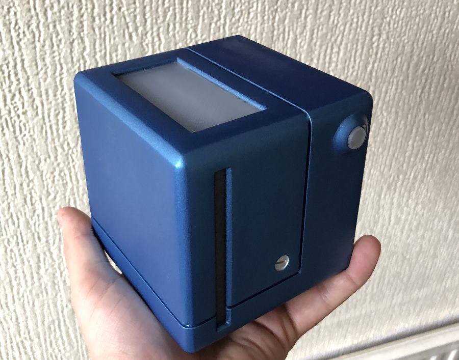
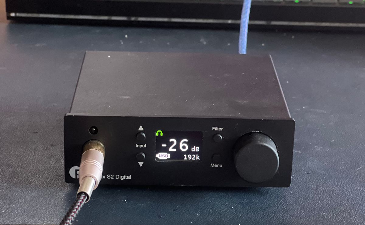
This is what happened to my "Pro-Ject Pre Box S2 Digital", it's a great little box that will take USB, Coax Digital or SPDIF as an input and output line level stereo out via RCA jacks on the back or amplified headphone output on the front - which is primarily what I use. The audio quality is excellent - it's beyond anything a PC motherboard would output.
The catch being, of course - the manufacturer ("Pro-Ject") decided they would use an OLED screen for the front panel. Sure new technology, great idea - looks A++.
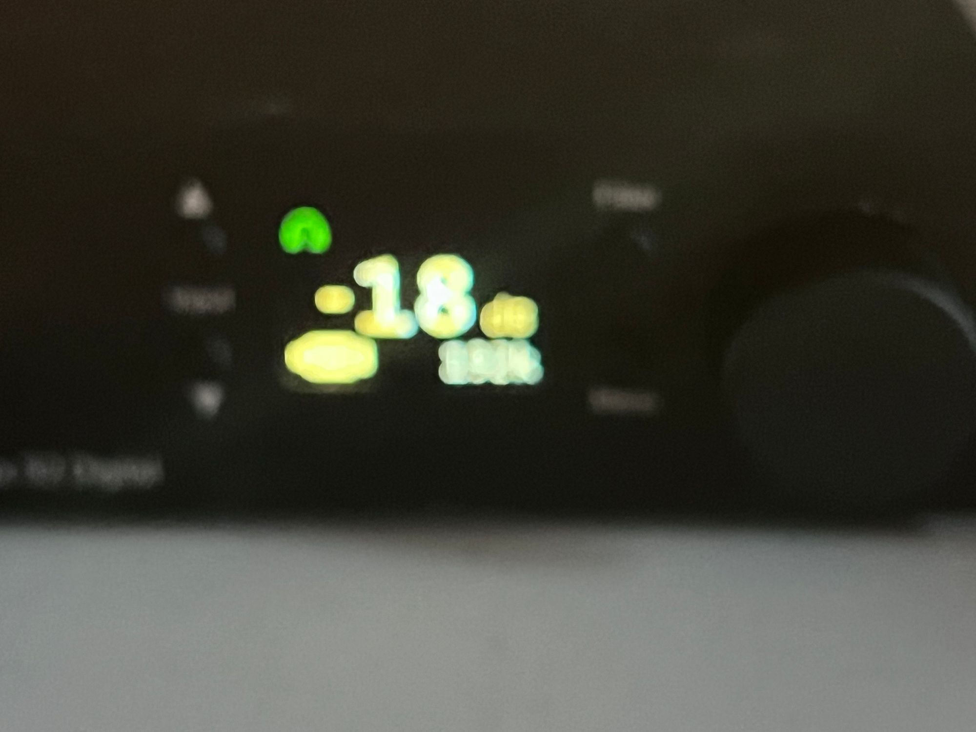
Except after less than a year's usage, the screen had burnt in for me. Granted, the device was practically never turned off, but still. Pro-Ject sadly did not add an OLED blanking feature to their firmware, and the screen doesn't even dim when idle.
This to me seems like an obvious omission - I fed back to Pro-Ject they should add this, and I received an acknowledgement for my feedback - but there's no new firmware. It also wouldn't help my unit that already has burnt - so, can I do anything about it? Out comes the screwdriver!
Repairing?
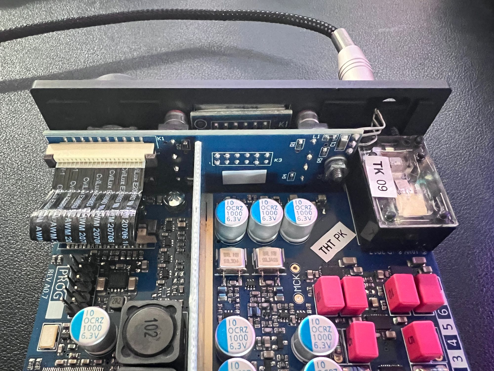
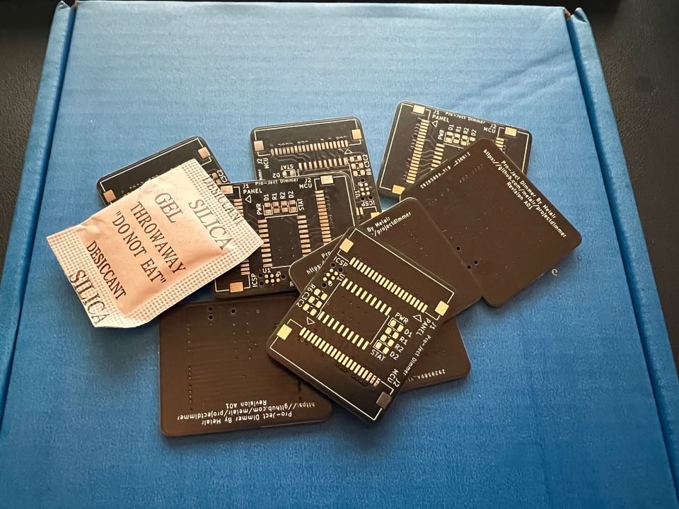
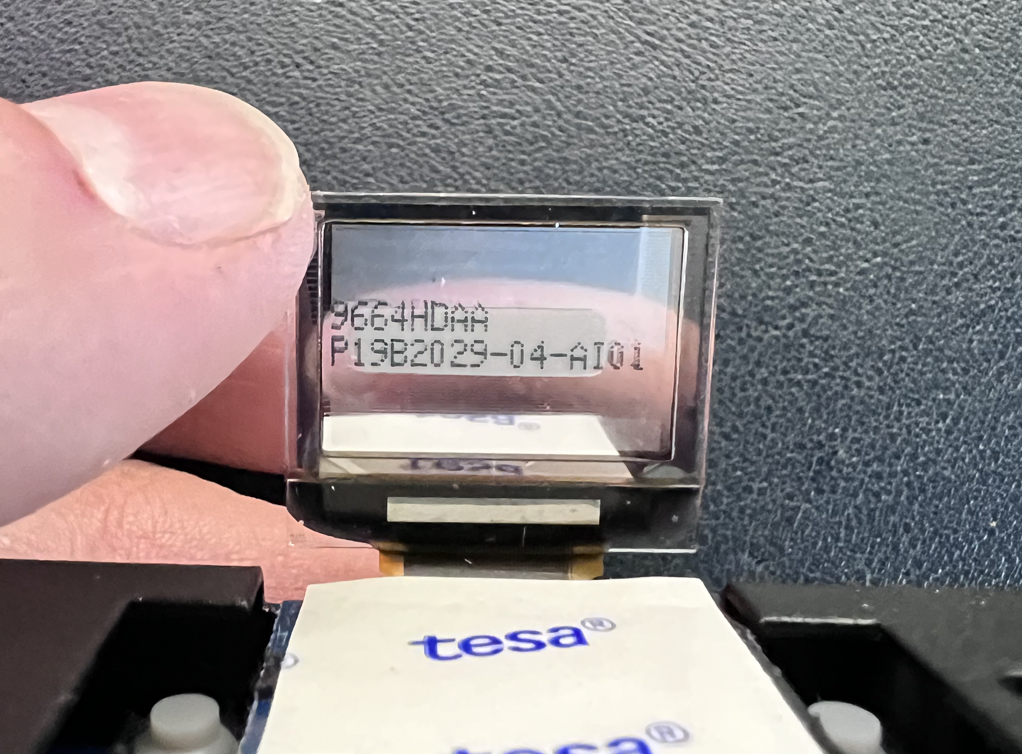
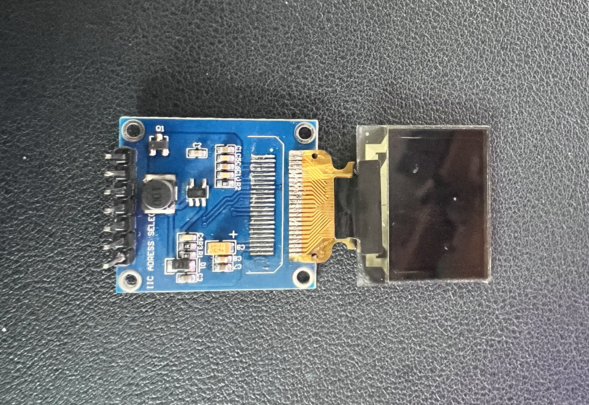
It turns out the OLED screen is 0.95" large, which seems suspiciously similar to the size easily available for hobbyist electronics. Doing more investigation, it appears to be a standard size and model, 9664HDAA. Searching the internet suggests that it should have the SSD1331 control chip.
To verify if it is, it's time to multimeter the back of the OLED display and figure out the purpose of each pin, looking for a VCC, GND, /CS, D/C, SCLK and COPI.
It used to be known as MOSI (Master Out, Slave In). In June 2020, the Open Source Hardware Association announced a resolution for changing how SPI was labelled.
As Sinclair Im of The Washington Post writes regarding software engineering, "Should an African American software developer be required to write code wherein a master process commands slaves?".
It's time we changed the language in our hobby/industry.
After some work, I found the obvious pins like VCC and GND quickly, but the data pins read as VCC in voltage measuring mode. Using continuity when the unit was off, I verified that they weren't connected directly to VCC, so they are likely pulled up to VCC - they read several megaohms to VCC when off (foreshadowing).
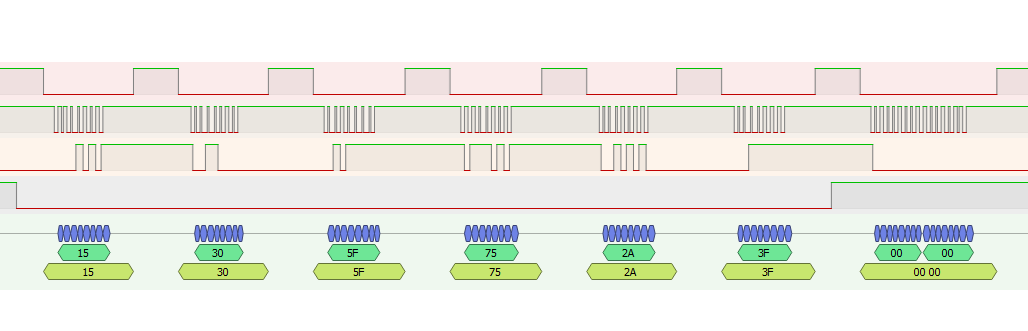
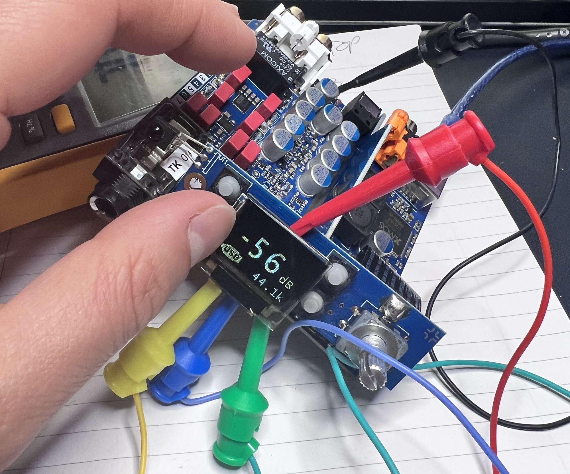
After a few aborted capture attempts, primarily due to being unable to run my logical analyser at 32MHz for a long time, I managed to capture the data. After referring to the SDD1311 manual, this appears to be a good couple of instructions. This gave me the drive to try and replace it - but first, let's test. It should be possible to drive both displays at once.
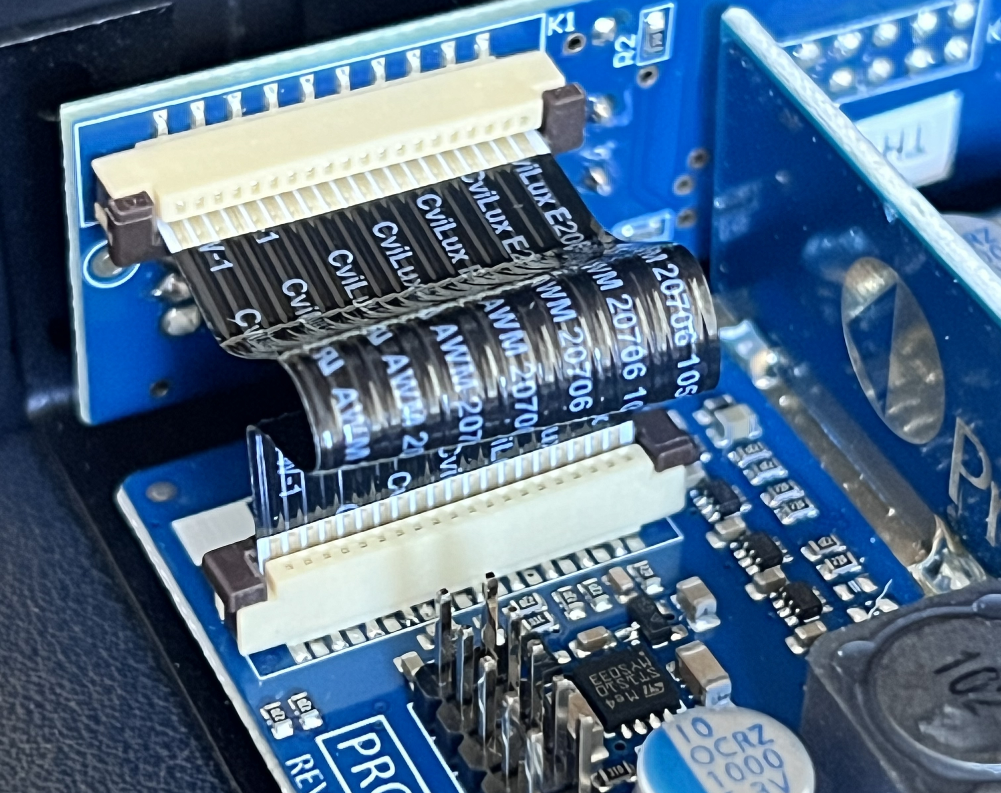
Welp - the test proved it. I figured out the connections correctly; it's the same protocol. Though I don't have a picture, the FPC cable on the back of the OLED display has the same number of connections and pitch.
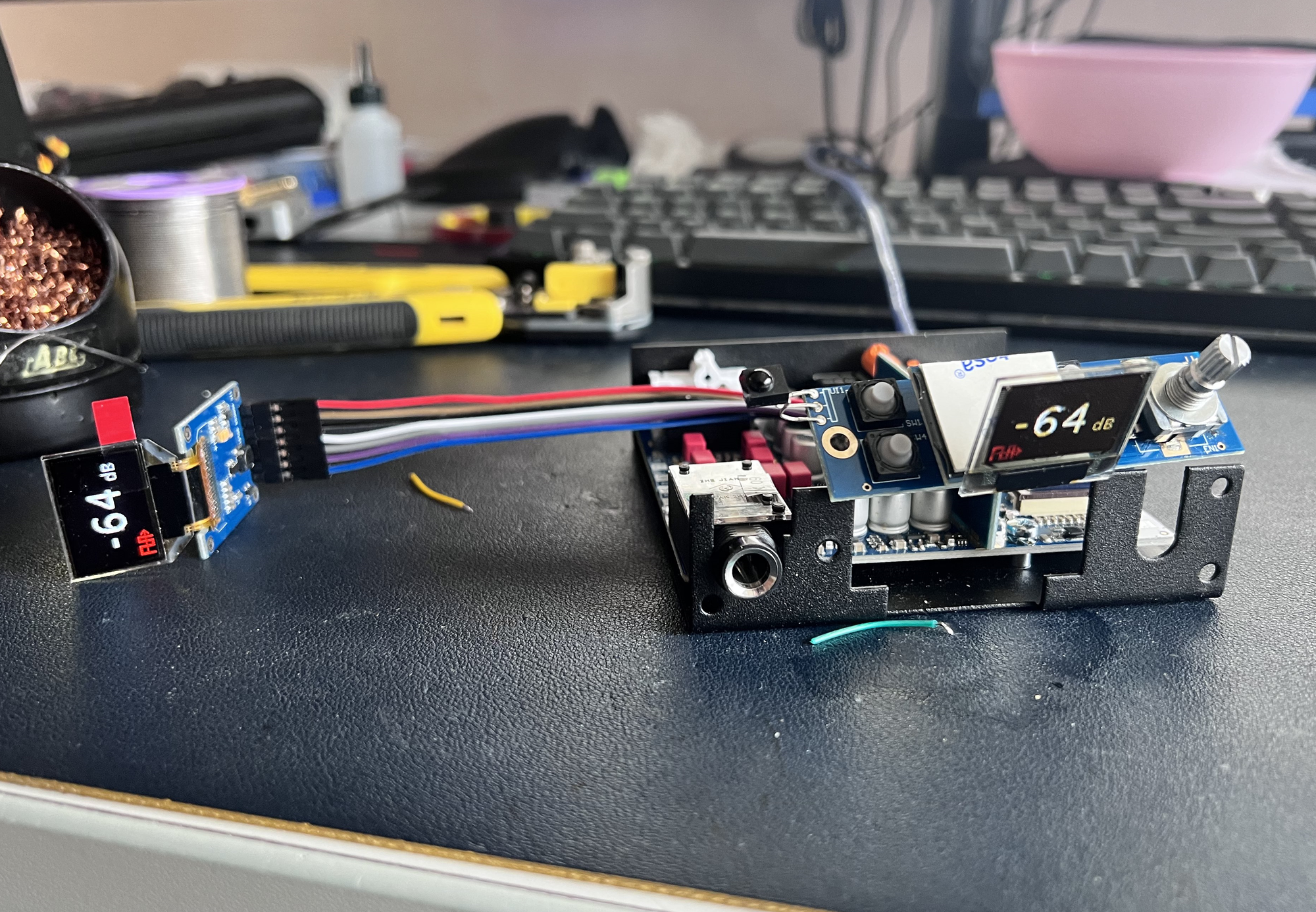
As shown by the splash image of this post, the transplant was a complete success - the display once again looked glorious. It only took about 20 minutes to swap it out - but having a solder removal station, good soldering iron and a hot air rework station make that much easier.
But won't it happen again?
Yes - yes, it will. I can keep replacing the OLED modules, but sooner or later, I won't be bothered, or I'll damage the pads on the OLED board of the DAC. My preferred solution is Pro-Ject sorting this out via firmware - but that doesn't seem likely; maybe this post will push them to. 🤷♂️
The SSD1311 has commands to lower the output power or blank the screen - that's the great thing about OLED. If the pixels are off - nothing is happening. It's not like TFT is blocking a backlight that's slowly fading.
So... what can I do? Can I mod the DAC? I could try the firmware hacking route - but a relatively obscure chip runs it that I've never seen before made by a company called XMOS. They seem ideal for audio processing work - which I've never done.
But the control of the OLED screen is just SPI - I should just be able to inject instructions into that. The idea would be that my mods would watch the /CS (chip select) line for the OLED display. I had already identified earlier that the screen was only updated on change. The mod would wait for X period after the /CS line was used and then inject the screen off command. Then after it'd seen the /CS line used, it would send the screen on command. Simple!
My first thought was if I could make a retro games console-style mod that was just soldered over the OLED 0.1" connectors.
First, I had to check how the SPI lines were driven to 3.3V. There are three common approaches:
- External Pull Up Resistor
- Internal (to XMOS microcontroller) Pull Up Resistor
- Push/Pull of the IO Pin
In the case of the external pull-up resistor, this was disproved earlier when I tested the data lines for resistance to VCC. It was above any sane value used for the pull-up. I read several megaohms; you'd usually use something in the order of 10k - I've used 47k several times.
Testing for an internal pull-up resistor was harder but could be done briefly using the multimeter in low-current measurement mode. So I did, and saw 34mA, using ohms law... that's a resistance of ~100 ohms. That's very low for a pull-up resistor; 34mA is a lot of current to sink.
I had a look for the particular XMOS chip datasheet the Pre Box used, but I couldn't find it - similar chips seem to claim to be able to source up to 30mA. So what does this mean? It's not an internal pull-up. It's likely the GPIO push/pull on the IO pin. Push/pull what you say?
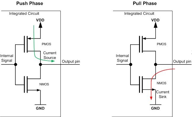
When an MCU wants to output a high signal on its IO pin, it connects that pin to VCC via a transistor. When it wants to output at a low signal, it connects it to GND by a transistor.
So why's this a problem? If my microcontroller wants to produce SPI signals, it has to make the SPI lines read low. Now the PIC18s I usually use can sink ~50mA - so it could do it, but it's not great for either chip, and the XMOS is likely to be damaged sourcing more than its limits.
Some communications protocols allow multiple controllers to control the bus or require the peripheral chips to be able to change the state of the wire (such as I²C).
A pull-up resistor ensures the chips don't have to sink too much current. It also means they only need half of a push/pull, only the pull - this is often known as open-drain.
Given I don't want to sink all of that current via my microcontroller, what else can we do? Well, how can we break the connection between the XMOS microcontroller and the OLED display?
Simple, I insert myself between the main board and the interface board. After much probing, I managed to reverse engineer the pinout (see below, where pin 1 is on the left-hand side).
| Pin | Purpose |
|---|---|
| 1 | GND |
| 2 | Unused (Probably, couldn't find it going anywhere on the interface board.) |
| 3 | GND |
| 4 | SPI CLK |
| 5 | GND |
| 6 | SPI COPI |
| 7 | 3.3V |
| 8 | SPI /CS |
| 9 | OLED /RES |
| 10 | OLED C/D |
| 11 | 12V (Used to drive OLED pixels) |
| 12 | Rotary Encoder A |
| 13 | Rotary Encoder B |
| 14 | Rotary Encoder Push |
| 15 | Button (Right Bottom) |
| 16 | Button (Right Top) |
| 17 | Button (Left Bottom) |
| 18 | Button (Left Top) |
| 19 | Infrared |
| 20 | GND |
Designing an interception board
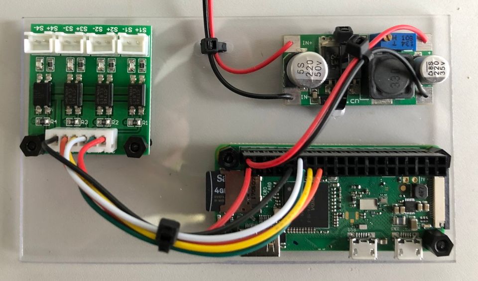
Due to over-ordering during COVID-19 and building up stocks of certain microchips, I'm slowly working through many PIC18F15Q40 (this is not a complaint).
You might be able to use DMA, but it would be tight. The PIC18F15Q40 can run at 64MHz, but each instruction takes four cycles - so 16 MIPS. Assuming the clocks aligned perfectly, you would have eight instructions between bytes.
I will test this once it is built.
As it happens, it's a 20-pin MCU with some features that will REALLLY help me on this project.
- Peripheral Pin Select
Essentially any hardware peripheral can be routed to any pin on the MCU - this means I don't have to care about pin assignments (bar two + VCC/GND). - Two SPI Peripherals
There is dedicated silicon for producing SPI signals. All I have to do is put data into registers, and it's sent out. - DMA Controllers
DMA controllers are dedicated hardware that moves data in memory, which doesn't sound helpful until you realise you can point the source at a buffer in RAM and the destination at a peripherals register. Then you can tell it to move data whenever a specific interrupt occurs.
Essentially this means you can send large SPI messages without your program code being involved other than to start the transaction. - Configurable Logic Cells
Given that the SPI bus is running at a very high baud rate, I'm not comfortable that I could receive, buffer and then send bytes to the OLED screen - I might even run out of RAM buffering.
So instead CLCs allow me to not have a bus switch chip on the intercept board to disconnect the XMOS. CLCs are logic gates that do not run on the MCUs clock, and they can be configured to be AND-OR, NOT, JK Flip Flops, etc.
As such, I can pass the XMOS raw SPI signal through the PIC18 while the interceptor is not issuing commands to the display but disconnect/block the XMOS while I am.
Because of all these features, the board is pretty simple.
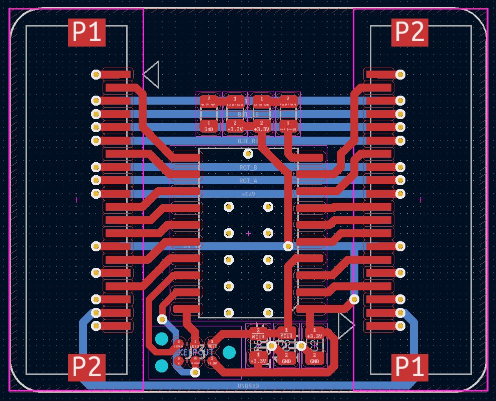
You can see that many lines are passed straight through, but just as many are routed to the microcontroller. The obvious ones for the OLED screen are, but I'm also intercepting the infrared signal.
By intercepting the infrared signal, I can read the pulses from the remote - which happens to have a "BAL" (for Balance) button, which is unused on this unit. I plan that pressing the BAL button will open a menu that allows you to adjust the timeouts and brightness of the display.
I might also put an easter egg game or similar in and take over the display.
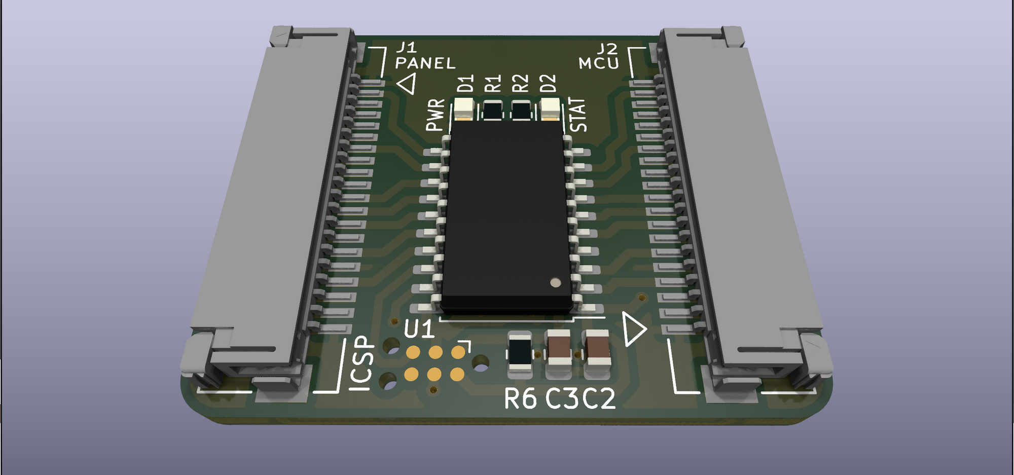
The board has been sent to manufacture, so part two of this post will come soon enough!